


TSMC To Experiment With “Rectangular Substrates”, Tripling Performance Through Higher Area Utilization
TSMC To Experiment With “Rectangular Substrates”, Tripling Performance Through Higher Area Utilization
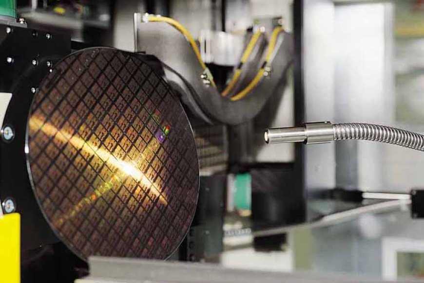
TSMC is looking to explore a revolutionary route in semiconductors by developing "advanced chip packaging" using rectangular substrates.
With the rapidly growing AI sector, the need for higher computational power has become more important than ever. While the industry employs techniques such as node shrinking and architectural gains, opting for innovative and new routes has become a necessity, and it looks like the Taiwan giant is doing just that. Nikkei Asia reports that TSMC is moving towards employing rectangular panel-like substrates, moving away from conventional wafer design techniques for higher wafer area utilization.
Now, what's the advantage of rectangular substrates? With this size, panels will have a larger usable area compared to circular wafers, allowing more chips to be placed on a single substrate.
The report says that rectangular substrates currently being experimented with are 510 millimeters by 515 millimeters, increasing the area by almost three times, which means higher efficiency and, ultimately, an advanced process. It also means there will be less unused area on wafers, which means less semiconductor wastage.
Despite the benefits, achieving rectangular substrates isn't easy since it requires superior chip stacking and assembly techniques and makes the manufacturing process much more complex, which currently is a barrier for TSMC. Changes in panel dimensions won't be required in the shorter term, but with the way the AI industry is evolving, industry standards will ultimately force firms like TSMC to come up with newer options. Hence, rectangular substrates are a technique that could be employed in the long run.
Commenting on the change, here's what an analyst from Bernstein Research had to say on the use of rectangular substrates:
This shift would require a significant overhaul of facilities, including upgrades to robotic arms, and automated material handling systems to process the different shapes of substrates.
This is likely a long-term plan spanning five to 10 years, not something achievable in the short term.
One advantage TSMC has here is how well the firm has established itself when it comes to finances. Since it has the confidence of customers such as NVIDIA, Amazon, AMD, and Google, opting for such techniques won't be a pain for the firm, at least economically. However, rectangular substrates are still a concept for now, and their execution will require more than just money.
News Source: Nikkei Asia
What's Your Reaction?


