


Samsung Looks To Reach Over 1000-Layer NAND Through Newly-Emerged Hafnia Ferroelectrics
Samsung Looks To Reach Over 1000-Layer NAND Through Newly-Emerged Hafnia Ferroelectrics
Samsung Electronics' plans to reach a "petabyte" storage goal seemed unrealistic a while ago, but the firm is now considering using new "ferroelectric" materials to achieve the goal potentially with over 1000-Layer NAND technology.
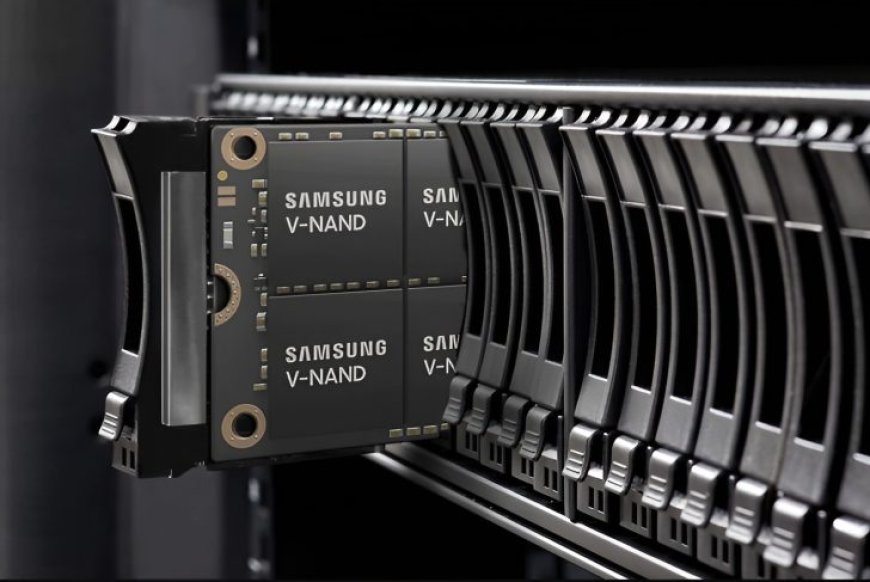
Recently, we talked about Samsung's plans for the future of the NAND markets, including the release of 9th Gen V-NAND flash, which will come with a whopping 290 layers stacked upon each other, setting a new market benchmark. Interestingly, the Korean giant also announced a NAND product with a shocking 430-layer stacking (10th Gen V-NAND) that is expected to launch next year. With such equipment onboard, Samsung Electronics plans to cross the 1000 TB milestone as soon as possible, but there's another exciting touch.
At the VLSI Technology Symposium in Honolulu, researchers from the Korea Advanced Institute of Science and Technology (KAIST) are expected to present their findings on Hafnia Ferroelectrics, which is a class of materials that exhibit ferroelectricity upon certain conditions. They have seen massive interest in recent times, especially from the computing industry, since their ferroelectric properties might enable the development of smaller, more efficient capacitors and memory devices.
Here is how the work to be presented is summarized based on initial details about the conference:
In-depth Analysis of the Hafnia Ferroelectrics as a Key Enabler for Low Voltage & QLC 3D VNAND Beyond 1K Layer Experimental Demonstration and Modeling
In this work, we experimentally demonstrate a remarkable performance improvement, boosted by the interaction of charge trapping & ferroelectric (FE) switching effects in metal-band engineered gate interlayer (BE-G.IL)-FE-channel interlayer (Ch.IL)-Si (MIFIS) FeFET. The MIFIS with BE-G.IL (BE-MIFIS) facilitates the maximized ‘positive feedback’ (Posi. FB.) of dual effects, leading to low operation voltage (VPGM/VERS: +17/-15 V), a wide memory window (MW: 10.5 V) and negligible disturb at a biased voltage of 9 V.
Furthermore, our proposed model verifies that the performance enhancement of the BE-MIFIS FeFET is attributed to the intensified posi. FB. This work proves that the hafnia FE can play as a key enabler in extending the technology development of 3D VNAND, which is currently approaching a state of stagnation.
- VLSI Technology Symposium
It's important to note that Samsung isn't directly involved in the R&D process, but the involved personalities are said to be directly related to the Korean giant. While it isn't sure whether Hafnia Ferroelectrics would lead to the creation of petabyte storage devices, they could play a dominant role, ultimately leading us to the milestone.
What's Your Reaction?


