


NVIDIA Blackwell GPU Architecture Official: 208 Billion Transistors, 5x AI Performance, 192 GB HBM3e Memory, 8 TB/s Bandwidth
NVIDIA Blackwell GPU Architecture Official: 208 Billion Transistors, 5x AI Performance, 192 GB HBM3e Memory, 8 TB/s Bandwidth
NVIDIA has officially unveiled its next-gen Blackwell GPU architecture which features up to a 5x performance increase versus Hopper H100 GPUs.
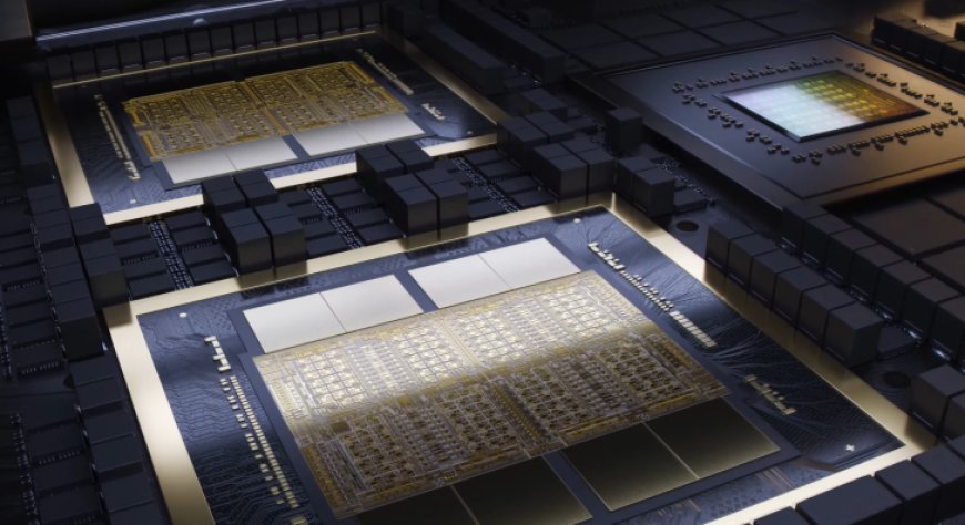
NVIDIA has gone official with the full details of its next-generation AI & Tensor Core GPU architecture codenamed Blackwell. As expected, the Blackwell GPUs are the first to feature NVIDIA's first MCM design which will incorporate two GPUs on the same die.
Diving into the details, the NVIDIA Blackwell GPU features a total of 104 Billion transistors on each compute die which is fabricated on the TSMC 4NP process node. Interestingly, both Synopsys and TSMC have utilized NVIDIA's CuLitho technology for the production of Blackwell GPUs which makes making Each chip accelerates the manufacturing of these next-gen AI accelerator chips. The B100 GPUs are equipped with a 10 TB/s high-bandwidth interface which allows super-fast chip-to-chip interconnect. These GPUs are unified as one chip on the same package, offering up to 208 Billion transistors and full GPU cache coherency.
Compared to the Hopper, the NVIDIA Blackwell GPU offers 128 Billion more transistors, 5x the AI performance which is boosted to 20 petaFlops per chip, and 4x the on-die memory. The GPU itself is coupled with 8 HBM3e stacks featuring the world's fastest memory solution, offering 8 TB/s of memory bandwidth across an 8192-bit bus interface and up to 192 GB HBM3e memory. To quickly sum up the performance figures versus Hopper, you are getting:
NVIDIA will be offering Blackwell GPUs as a full-on platform, combining two of these GPUs which is four compute dies with a singular Grace CPU (72 ARM Neoverse V2 CPU cores). The GPUs will be inter-connected to each other and the Grace CPUs using a 900 GB/s NVLINK protocol.
First up, we have the NVIDIA Blackwell B200 GPU. This is the first of the two Blackwell chips that will be adopted into various designs ranging from SXM modules, PCIe AICs & Superchip platforms. The B200 GPU will be the first NVIDIA GPU to utilize a chiplet design, featuring two compute dies based on the TSMC 4nm process node.
MCM or Multi-Chip-Module has been a long coming on the NVIDIA side of things &it's finally here as the company tries to tackle challenges associated with next-gen process nodes such as yields and cost. Chiplets provide a viable alternative where NVIDIA can still achieve faster gen-over-gen performance without compromising its supply or costs and this is just a stepping stone in its chiplet journey.
The NVIDIA Blackwell B200 GPU will be a monster chip. It incorporates a total of 160 SMs for 20,480 cores. The GPU will feature the latest NVLINK interconnect technology, supporting the same 8 GPU architecture and a 400 GbE networking switch. It's also going to be very power-hungry with a 700W peak TDP though that's also the same as the H100 and H200 chips. Summing this chip up:
On the memory side, the Blackwell B200 GPU will pack up to 192 GB of HBM3e memory. This will be featured in eight stacks of 8-hi modules, each featuring 24 GB VRAM capacity across an 8192-bit wide bus interface. This will be a 2.4x increase over the H100 80 GB GPUs which allows the chip to run bigger LLMs.
The NVIDIA Blackwell B200 and its respective platforms will pave a new era of AI computing and offer brutal competition to AMD and Intel's latest chip offerings which are yet to see widespread adoption. With the unveiling of Blackwell, NVIDIA has once again cemented itself as the dominant force of the AI market.
What's Your Reaction?


