NVIDIA Blackwell GB202 Gaming GPUs To Utilize TSMC 4NP Node, Significant Improvement To Cache & SM Throughput
NVIDIA Blackwell GB202 Gaming GPUs To Utilize TSMC 4NP Node, Significant Improvement To Cache & SM Throughput
NVIDIA just announced its Blackwell GPUs for AI and now eyes are all set on its gaming parts which are rumored to feature the same TSMC 4NP node.
It was previously expected that NVIDIA was going to leverage the TSMC 3nm process node for the gaming chip but that plan has seemingly changed as Kopite7kimi now states both Blackwell AI Tensor Core and Gaming GPUs to be fabricated on a very similar process node. Just a few hours ago, we came to know that NVIDIA will be using TSMC's 4NP node, a variation of the 5nm node that was already used for Ada Lovelace and Hopper GPUs.
It is stated that the new process node will allow a 30% increase in transistor density which can lead to higher performance gains but the actual efficiency advantages are yet to be explained. TSMC doesn't explicitly state the 4NP process node anywhere on its webpage. They only mention N4P & which is also mentioned as an extension of the N5 platform with an 11% performance boost over N5 and a 6% boost over N4.
GB202 will use the same process node as GB100. I must clarify once again that TSMC 4N(vidia) is based on TSMC 5, not 4nm. I'm sorry I cannot match Jensen's naming with TSMC's naming. We need professional chip analysis to determine. At least, there is a 30% increase in density.
— kopite7kimi (@kopite7kimi) March 19, 2024
We know that the previously used 4N process node for Ada GPUs was simply N5 (5nm) in disguise with some NVIDIA-exclusive optimizations. NVIDIA also revealed that it has worked with TSMC and Synopsys to leverage the game-changing CuLitho technology to make sure that the production and manufacturing of these new-gen Blackwell AI Tensor & Gaming GPUs go smoothly so that they can be delivered to customers on time.
https://twitter.com/kopite7kimi/status/1769898435367620933
Other than the process node, NVIDIA is also expected to deliver some big gains on the L1 cache side. It is stated that GB202, the flagship Blackwell Gaming GPU, will have significant improvements versus AD102 and GA102 which will allow the increase in SM throughput. Kopite7kimi also shed some light on the configuration of Blackwell GB202 Gaming GPU earlier.
He stated that the chip is going to offer 12 GPCs, each with 8 TPCs for a total of 96 TPCs and if we take into account the Ada structure, we can expect up to 192 SMs or 24,567 CUDA cores assuming that there will be 128 FP32 cores per SM. That's going to be 33% more CUDA cores than the full AD102 GPU which so far hasn't been released.
As I mentioned before, GA100 is 8*8, and GH100 is 8*9. GB100 will have a basic structure like 8*10. GB202 looks like 12*8.
— kopite7kimi (@kopite7kimi) September 28, 2023
I think GB203 is half of GB202, just like GB102 and GB100. But I don't know if GB202 has a multi chip package.
— kopite7kimi (@kopite7kimi) March 11, 2024
He also mentions that the GB203 GPU, the next in the Blackwell Gaming GPU lineup, will be half of the GB202, similar to AD102 and AD103 GPUs. This will lead to a huge disparity in performance if NVIDIA equips the next 90-series cards with GB202 and the 80-series cards with GB203. The biggest question is whether NVIDIA will utilize MCM (Multi-Chip-Module) packaging for its Blackwell Gaming GPUs or keep them monolithic for now. Given the increasing costs and yield issues associated with GPU/chip development, the chiplet route is indeed the way of the future & AMD's Radeon division has already embraced it.
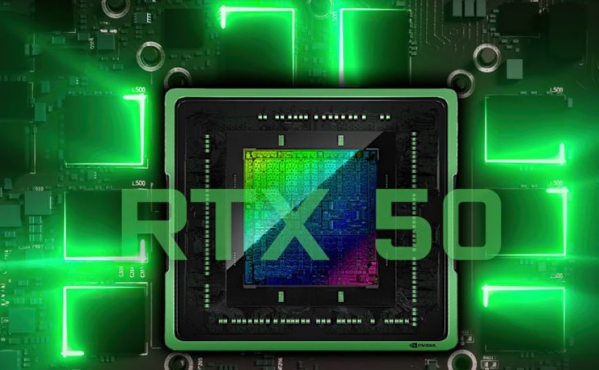
NVIDIA's Blackwell Gaming GPUs will launch under the GeForce RTX 50 series family with the support of next-gen technologies such as GDDR7 memory, DisplayPort 2.1, and more. We can expect to hear more about them later this year.
What's Your Reaction?