


Intel Teases Meteor Lake 5-125W Core CPUs With Up To 192 EU GPU, 12th Gen Alder Lake Hinted For 27th October Launch
Intel Teases Meteor Lake 5-125W Core CPUs With Up To 192 EU GPU, 12th Gen Alder Lake Hinted For 27th October Launch
Intel has teased its next-generation Meteor Lake CPUs during the IDM 2.0 Accelerated keynote where the company presented its brand new process and packaging roadmap. In addition to the teaser, Intel also hinted at a possible launch date of its upcoming Alder Lake hybrid CPUs during early Q4 2021.
Intel not only presented its brand new process and packaging roadmap but also teased products that will be utilizing its new nodes, mainly Intel 7 and Intel 4. First up, we have Alder Lake Client & Sapphire Rapids Data Center chips which will be based upon the Intel 7 node (previously Intel 10 Enhanced SuperFin).
Based on what Intel showed during the event, it looks like we can confirm that the leaks we have seen so far are more or less confirmed. The Alder Lake CPU can be seen using a hybrid design & features 8 high-performance cores (Golden Cove) and 8 efficiency optimized cores (Gracemont). Intel also kind of hinted at the launch date of its 12th Gen Alder Lake family for 27th October and that aligns with earlier rumors that we heard about the CPUs launching around Halloween 2021. The next Intel ON series event will take place virtually in San Francisco on October 27-28, 2021.
Moving on, we have Intel's Sapphire Rapids-SP Xeon CPU which is composed of four compute tiles. We have more detailed images of the complete die leak out before which confirm up to 56 cores & 112 threads.
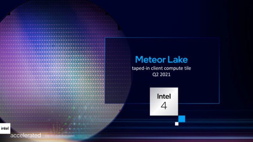
Intel 4 will also power two key client and data center products which are codenamed Meteor Lake & Granite Rapids. This is the first time Intel has given a detailed look at the Meteor Lake SOC that features three separate chiplets that are connected together through Forveros technology. Intel is expected to utilize a next-generation core architecture that will power the compute die while the I/O will be located on its own SOC-LP die. The GPU die will also be separate and will be composed of up to 192 EU (96 EU for Desktops & 192 EUs for Mobility). The Meteor Lake lineup will comprise 5-125W CPUs and feature a bump pitch of 36u (microns).
We already got some details from Intel such as the fact that Intel's Meteor Lake line of desktop and mobility CPUs are expected to be based on a new line of Cove core architecture. This is rumored to be known as the 'Redwood Cove' and will be based on a 7nm EUV process node. It is stated that the Redwood Cove is designed from the ground up to be an agnostic node which means that it can be fabricated at different fabs. There are references mentioned that point out to TSMC to be a backup or even a partial supplier for the Redwood Cove-based chips. This might tell us why Intel is stating multiple manufacturing processes for the CPU family.
The Meteor Lake CPUs may possibly be the first CPU generation from Intel to say farewell to the ring bus interconnect architecture. There are also rumors that Meteor Lake could be a fully 3D-Stacked design and could utilize an I/O die sourced from an external fab (TSMC sighted again). It is highlighted that Intel will be officially utilizing its Foveros Packaging Technology on the CPU to inter-connect the various dies on the chip (XPU). This also aligns with Intel referring to each tile on 14th Gen chips individually (Compute Tile = CPU Cores).
The Meteor Lake Desktop CPU family is expected to retain support on the LGA 1700 socket which is the same socket used by Alder Lake & Raptor Lake processors. We can expect DDR5 memory and PCIe Gen 5.0 support. The platform will support both DDR5 & DDR4 memory with the mainstream and budget tier options going for DDR4 memory DIMMs while the premium & high-end offerings going for DDR5 DIMMs. The site also lists down both Meteor Lake P and Meteor Lake M CPUs that will be aimed at mobility platforms.
Intel has also showcased its next-generation Granite Rapids datacenter Xeon CPU which seems to be featuring several dies packaged through Forveros and EMIB. We can see HBM packages along with high-bandwidth Rambo Cache packages. The Compute tile seems to be composed of 60 cores per die which equals 120 cores in total but we should expect a few of those cores to be disabled to get better yields on the new Intel 4 process node.
What's Your Reaction?


