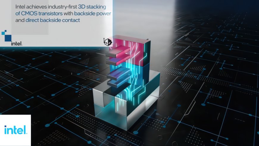
Intel is demonstrating its next-gen 3D Stacked CMOS Transistor technology which utilizes backside power & direct backside contact to deliver more performance and scaling on next-gen chips.
Press Release: Today, Intel unveiled technical breakthroughs that maintain a rich pipeline of innovations for the company’s future process roadmap, underscoring the continuation and evolution of Moore’s Law.
At the 2023 IEEE International Electron Devices Meeting (IEDM), Intel researchers showcased advancements in 3D stacked CMOS (complementary metal oxide semiconductor) transistors combined with backside power and direct backside contacts. The company also reported on scaling paths for recent R&D breakthroughs for backside power delivery, such as backside contacts, and it was the first to demonstrate successful large-scale 3D monolithic integration of silicon transistors with gallium nitride (GaN) transistors on the same 300-millimeter (mm) wafer, rather than on the package.
“As we enter the Angstrom Era and look beyond five nodes in four years, continued innovation is more critical than ever. At IEDM 2023, Intel showcases its progress with research advancements that fuel Moore’s Law, underscoring our ability to bring leading-edge technologies that enable further scaling and efficient power delivery for the next generation of mobile computing.”
–Sanjay Natarajan, Intel senior vice president and general manager of Components Research
“As we enter the Angstrom Era and look beyond five nodes in four years, continued innovation is more critical than ever. At IEDM 2023, Intel showcases its progress with research advancements that fuel Moore’s Law, underscoring our ability to bring leading-edge technologies that enable further scaling and efficient power delivery for the next generation of mobile computing.”
Why It Matters: Transistor scaling and backside power are key to helping meet the exponentially increasing demand for more powerful computing. Year after year, Intel meets this computing demand, demonstrating that its innovations will continue to fuel the semiconductor industry and remain the cornerstone of Moore’s Law. Intel’s Components Research group consistently pushes the boundaries of engineering by stacking transistors, taking backside power to the next level to enable more transistor scaling and improved performance, as well as demonstrating that transistors made of different materials can be integrated on the same wafer.
The image at left shows a design with power and signal wires intermingled on the top of the wafer. The image at right shows the new PowerVia technology, Intel’s unique industry-first implementation of a backside power delivery network. PowerVia was introduced at the "Intel Accelerated" event on July 26, 2021. At the event, Intel presented the company's future process and packaging technology roadmaps. (Credit: Intel Corporation)
Recent process technology roadmap announcements highlighting the company’s innovation in continued scaling – including PowerVia backside power, glass substrates for advanced packaging and Foveros Direct – originated in Components Research and are expected to be in production this decade.
How We Do It: At IEDM 2023, Components Research showed its commitment to innovating new ways of putting more transistors on silicon while achieving higher performance. Researchers have identified key R&D areas necessary to continue scaling by efficiently stacking transistors. Combined with backside power and backside contacts, these will be major steps forward in transistor architecture technology. Along with improving backside power delivery and employing novel 2D channel materials, Intel is working to extend Moore’s Law to a trillion transistors on a package by 2030.
Intel delivers industry-first, breakthrough 3D stacked CMOS transistors combined with backside power and backside contact:
Intel’s latest transistor research presented at IEDM 2023 shows an industry first: the ability to vertically stack complementary field effect transistors (CFET) at a scaled gate pitch down to 60 nanometers (nm). This allows area efficiency and performance benefits by stacking transistors. It is also combined with backside power and direct backside contacts. It underscores Intel’s leadership in gate-all-around transistors and showcases the company’s ability to innovate beyond RibbonFET, putting it ahead of the competition.
Intel goes beyond five nodes in four years and identifies key R&D areas needed to continue transistor scaling with backside power delivery:
Intel’s PowerVia will be manufacturing-ready in 2024, which will be the first implementation of backside power delivery. At IEDM 2023, Components Research identified paths to extend and scale backside power delivery beyond PowerVia, and the key process advances required to enable them. In addition, this work also highlighted the use of backside contacts and other novel vertical interconnects to enable area-efficient device stacking.
Why It Matters: Transistor scaling and backside power are key to helping meet the exponentially increasing demand for more powerful computing. Year after year, Intel meets this computing demand, demonstrating that its innovations will continue to fuel the semiconductor industry and remain the cornerstone of Moore’s Law. Intel’s Components Research group consistently pushes the boundaries of engineering by stacking transistors, taking backside power to the next level to enable more transistor scaling and improved performance, as well as demonstrating that transistors made of different materials can be integrated on the same wafer.
Recent process technology roadmap announcements highlighting the company’s innovation in continued scaling – including PowerVia backside power, glass substrates for advanced packaging and Foveros Direct – originated in Components Research and are expected to be in production this decade.
How We Do It: At IEDM 2023, Components Research showed its commitment to innovating new ways of putting more transistors on silicon while achieving higher performance. Researchers have identified key R&D areas necessary to continue scaling by efficiently stacking transistors. Combined with backside power and backside contacts, these will be major steps forward in transistor architecture technology. Along with improving backside power delivery and employing novel 2D channel materials, Intel is working to extend Moore’s Law to a trillion transistors on a package by 2030.
Intel delivers industry-first, breakthrough 3D stacked CMOS transistors combined with backside power and backside contact:
Intel’s latest transistor research presented at IEDM 2023 shows an industry first: the ability to vertically stack complementary field effect transistors (CFET) at a scaled gate pitch down to 60 nanometers (nm). This allows area efficiency and performance benefits by stacking transistors. It is also combined with backside power and direct backside contacts. It underscores Intel’s leadership in gate-all-around transistors and showcases the company’s ability to innovate beyond RibbonFET, putting it ahead of the competition.
Intel goes beyond five nodes in four years and identifies key R&D areas needed to continue transistor scaling with backside power delivery:
Intel’s PowerVia will be manufacturing-ready in 2024, which will be the first implementation of backside power delivery. At IEDM 2023, Components Research identified paths to extend and scale backside power delivery beyond PowerVia, and the key process advances required to enable them. In addition, this work also highlighted the use of backside contacts and other novel vertical interconnects to enable area-efficient device stacking.