


SK Hynix Preparing NAND With ‘400-Layers’ Through Hybrid Bonding, 321-Layer NAND Shipping In 1H 2025
SK Hynix Preparing NAND With ‘400-Layers’ Through Hybrid Bonding, 321-Layer NAND Shipping In 1H 2025
SK Hynix aims for mass production to start its 400-layer NAND at the end of 2025 while 321-layer NAND hits production in 1H 2025.
The need for higher storage capacity is never ending and looks like SK Hynix is aiming at breaking its records with its new plan to prepare a 400-layer NAND for the future storage drives. Etnews reports that the company wants to start the mass production of this 400-layer NAND by the end of 2025 and wants to transition to full-scale production in the first half of 2026.
However, the process of creating such a high-layer NAND is complicated and requires several technologies for bonding. SK Hynix is already in the review process of the new materials for bonding and looking at various technologies that will allow connecting different wafers via methods like polishing, etching, deposition, and wiring.
The complete process requires several steps like cell structure design that focuses on the arrangement of cells in each layer and the stacking. The silicon wafers are then prepared by cleaning and applying thin layers of SiO2 and Si3N4. The process, however, needs careful execution when the layers are stacked one by one through a lot of repetition.
SK Hynix has already achieved a 321-layer NAND, which it showcased in August 2023, and plans to begin mass production in 1H 2025. With 400 layers, this will be the company's first and most advanced NAND product. Nonetheless, SK Hynix isn't the only player in the game. Memory giants such as Samsung and Micron are also in the process of increasing layers in their NAND chips. While Micron has recently introduced a dense NAND with 276 layers, Samsung has started mass production of a triple-level cell, 9th-gen vertical NAND, featuring 290 layers.
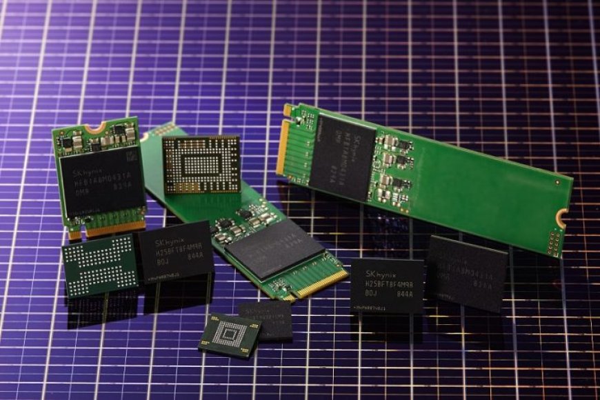
At FMS 2024, SK hynix will display the samples of the next-generation AI memory products such as the 12-layer HBM3E, expected to be mass produced in the third quarter, and 321-high NAND planned to be shipped from the first half of next year.
via SK hynix
Samsung is still aiming higher and is looking forward to producing NAND with over 1000 layers by 2030. That said, the Japanese company Kioxia is currently at 218 3D NAND layers with plans of achieving 1000 layers before Samsung.
SK Hynix's approach for reaching 400 layers is stacking the cells on top of the peripherals through the Peripheral Under Cell method. While the peripheral circuits, which control the memory cells are at the bottom, the memory cells are stacked on the top. This method does pose a problem of damaging the peripheral circuits as adding the layers generates more heat and pressure.
Therefore, the company is planning to implement the hybrid bonding method, which involves manufacturing the memory cells and peripheral circuits on separate wafers. Then the wafers will be bonded together to reduce the risk of damage. Through high layer count, the NAND chips can store a lot more data without increasing in size. This not only saves space for compact systems and increases the storage capacity but also results in more affordable storage solutions.
News Source: Etnews
What's Your Reaction?


