


SK Hynix Plans On Integrating GPU & Memory Semiconductors Into a Single Package, Defying Industry Trends
SK Hynix Plans On Integrating GPU & Memory Semiconductors Into a Single Package, Defying Industry Trends
The Korean memory manufacturer SK Hynix has decided to break from the industry's tradition of semiconductor development, as they plan to integrate memory and logic semiconductors on the same die.
According to reports by Korean outlets, SK Hynix believes there is a possibility of a more "efficient" implementation of semiconductor placements in the market, which the firm believes they can achieve with next-gen HBM4 memory. It is said that SK Hynix has hired a considerable number of design experts for logic semiconductors, which in the first place didn't make sense since the company solely focuses on memory, but with today's development, it seems like SK Hynix wants it to take on the semiconductor markets. What has prompted SK Hynix for a "rapid" change in the ecosystem? Well, we will discuss this later on.
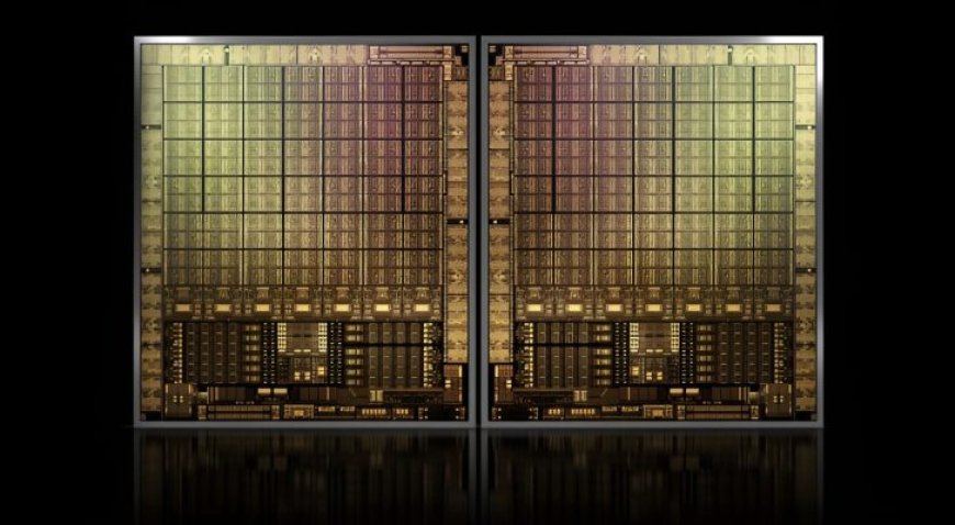
Regarding current-gen products, advanced memory semiconductors such as HBM are achieving efficiency by attaching them as closely as possible next to GPU chips, which are logic semiconductors. Individual computations are separated through a dedicated chip, which, in broader terms, does look like an inefficient method. Packaging techniques such as the CoWoS come in handy to bridge the gap between the semiconductors. However, some sort of "disparity" is still present, which is now intended to be catered by integrated memory and logic semiconductors into a single piece.
Moving on to why SK Hynix desires such implementation, it is simple. Currently, the semiconductor ecosystem order is divided into chip design (fabless), consignment production (foundry), and memory/logic. This not only involves sophisticated equipment for each manufacturing process, but in most cases, the work has to be outsourced to different firms specializing in their stages of development. A major drawback behind this is the "increased" reliance on individual firms, which has been evident in modern times in terms of huge order backlogs, which slows down the overall retailing process. Since firms like NVIDIA intend to pace up the manufacturing to-delivery process, reducing dependencies on each other is a primary factor in achieving the end goal.
It hasn't been revealed how SK Hynix plans on integrating logic and memory semiconductors into a single package, but sources say that SK Hynix is known to be discussing the HBM4 design method with several global fabless companies, including NVIDIA. We could see some sort of a "joint design" from the involved firms, which would act as a breakthrough in terms of computational performance as well as speeding up the overall manufacturing process, which is a vital need for modern times.
Based on history, process shrinking was seen as the only way to achieve generational gains, as validated by Moore's Law, but it looks like the future isn't wholly dependent on it. It is said that the semiconductor/memory industry could see a "megaton-level wave" that could cross all boundaries defined by current-gen limitations if firms can pull off the above-discussed idea. The future holds plenty for everyone, and it will be exciting to see how firms pave the way towards next-gen performance.
News Source: Joongang
What's Your Reaction?


