


Samsung Shows Off In-Memory Processing For HBM2, GDDR6 And Other Memory Standards
Samsung Shows Off In-Memory Processing For HBM2, GDDR6 And Other Memory Standards
Samsung announced they are planning to expand their innovative processing-in-memory tech to more HBM2 chipsets, but also DDR4, GDDR6 and LPDDR5X chipsets for the future of the memory chip technology. This information is in light of earlier this year when they reported to be producing HBM2 memory that utilizes an integrated processor that runs computations as high as 1.2 TFLOPS that can be manufactured for AI workloads, something that only CPUs, FPGAs, and graphics cards ASICs are usually expected to complete. This maneuver by Samsung will allow them to pave a spot in the near future for it's next generation HBM3 modules.
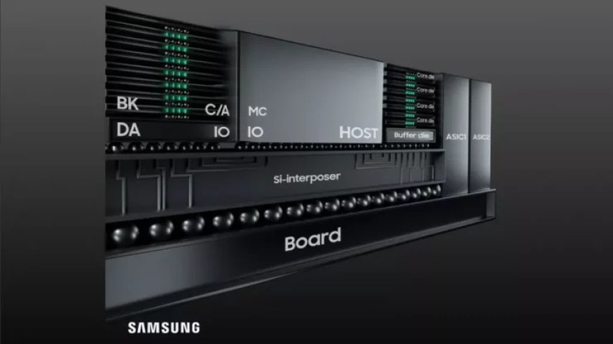
Put simply, the chips have an AI engine injected inside each DRAM bank. That allows the memory itself to process data, meaning that the system doesn't have to move data between the memory and the processor, thus saving both time and power. Of course, there is a capacity tradeoff for the tech with current memory types, but Samsung says that HBM3 and future memories will have the same capacities as normal memory chips.
— Tom's Hardware
Samsung's current Aquabolt-XL HBM-PIM fixtures itself into place, working side-by-side with their atypical JEDEC-compliant HBM2 controllers and allows for a drop-in structure, something that the current HBM2 standard does not allow. This concept was demonstrated by Samsung recently when they replaced the HBM2 memory into the Xilinx Alveo FPGA card with absolutely no modifications made. The process showed that the system's performance improved 2.5 times its normal functionality and a reduced consumption in energy of sixty-two percent.
The company is currently in the testing phase of the HBM2-PIM with a mysterious CPU vendor to help produce products in the next year. Unfortunately, we can only speculate that it would be with Intel and their Sapphire Rapids architecture, AMD and their Genoa structure, or Arm and their Neoverse models, only due to them all supporting HBM memory modules.
Samsung is staking claim to the technology moving forward, thanks to their AI workloads, dependent on increased memory structure with less formulaic computations in the programming, which is ideal for such areas of need like data centers. In return, Samsung exhibited it's new accelerated DIMM prototype, the AXDIMM. The AXDIMM computes all the processing straight from the buffer chip module. It is capable of showcasing the PF16 processors using TensorFlow measures as well as Python coding, but even the company is attempting to support other coding and applications as well.
The tests being constructed by Samsung using Zuckerberg's Facebook AI workloads showed almost two times the increase in computational performance and almost 43% energy reduction. Samsung also exclaimed that their tests showed a 70% tail latency reductions utilizing a two-rank kit, a phenomenal feat due to Samsung placing the DIMM chips into an atypical server and did not have to complete any modifications.
Samsung continues to experiment with PIM memory utilizing LPDDR5 chipsets, seen in more mobile devices and will continue into the following years. Aquabolt-XL HBM2 chipsets are currently in integration and available for purchase.
Source: Tom's Hardware
What's Your Reaction?


