


NVIDIA GeForce RTX 5090 GPU To Feature A Massive Monolithic GB202 “Blackwell” Die
NVIDIA GeForce RTX 5090 GPU To Feature A Massive Monolithic GB202 “Blackwell” Die
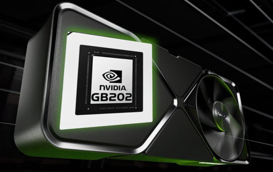
NVIDIA's GeForce RTX 5090 flagship GPU is going to feature a massive & monolithic GB202 "Blackwell" die, reports Kopite7kimi.
Based on what we know so far, the NVIDIA GB202 "Blackwell" GPU is going to power the flagship GeForce RTX 5090 graphics card. Preliminary specifications have revealed up to 192 SMs that will account for up to 24,567 CUDA cores if the chip retains the 128 cores per SM design from AD102 "Ada" chips. Now based on a new tweet from insider, Kopite7kimi, it is revealed that the GPU will be using a monolithic design.
physically monolithic
— kopite7kimi (@kopite7kimi) May 23, 2024
While NVIDIA has shifted to a chiplet design for its HPC/AI chips such as the B100 and B200, it will seem like the company still wants to retain the monolithic packages for its consumer-oriented GPU dies. It is said that the GB202 "Blackwell" GPU will be physically monolithic in design and from the earlier reports, we know that it is expected to feature twice the number of SMs and cores as GB203 which is a more cut-down die for the likes of the GeForce RTX 5080. That will form a huge disparity in the performance between the two cards but the RTX 5090 is shaping up to be a complete beast.
We will get to more on the NVIDIA GeForce RTX 5090 in a bit but before that, let's talk a bit more about the GB202 "Blackwell" GPU itself. So it looks like we are looking at a monolithic design but we also can't rule out the possibility of a chiplet-esque design under the hood.
NVIDIA may essentially be packing two GB203 dies on a monolithic package without making it seem like a chiplet design. It will allow for better inter-die communication rather than off-die communication bottlenecks associated with proper chiplet implementations. While NVIDIA has solutions to overcome the bottlenecks such as NVLINK and other interconnects, they might get a little bit expensive as they add to to the complexity of the GPU.
Four years ago, we split GA100 into two halves that communicate through an interconnect. It was a big move - and yet barely anyone noticed, thanks to amazing work from CUDA and the GPU team.
Today, that work comes to fruition with the Blackwell launch. Two dies. One awesome GPU. https://t.co/XuaUQPskkM pic.twitter.com/svRKhwPYEn
— Bryan Catanzaro (@ctnzr) March 18, 2024
NVIDIA already has a solution though which has already been out in the market in the form of the GA100 and GH100 which are essentially two halves of a smaller die connected with an interconnect and communicate through a split L2 cache. NVIDIA's Bryan Catanzaro explained that this implementation improves scalability and their initial transition to this design went smoothly. The chip is also expected to be based upon the TSMC 4NP process node (5nm) which improves density by 30% (transistor) so that oughta bring a nice improvement too besides the architectural upgrade.
Now, NVIDIA is probably going to do the same on the gaming side of things which means that if the whole thing pays off, then we can see a B100/B200 style chiplet offering in the future.
Now back to the NVIDIA GeForce RTX 5090, there are now multiple reports that we might be getting a 512-bit interface on the next-gen flagship and there is already information surrounding a brand new cooling and PCB solution in the works for this monster of a card.
Considering that rumors are suggesting AMD backing out of the ultra-high-end graphics performance segment with its RDNA 4 lineup, it looks like NVIDIA might further push its lead in the gaming segment with Blackwell GPUs once they hit the road. The NVIDIA GeForce RTX 5090 is expected to launch a few weeks apart from the RTX 5080 which is rumored to be the first Blackwell gaming GPU on shelves.
What's Your Reaction?


