


NVIDIA A100 80GB PCIe Accelerator Launched – Flagship Ampere Gets 2 TB/s Bandwidth For New HGX A100 Systems
NVIDIA A100 80GB PCIe Accelerator Launched – Flagship Ampere Gets 2 TB/s Bandwidth For New HGX A100 Systems
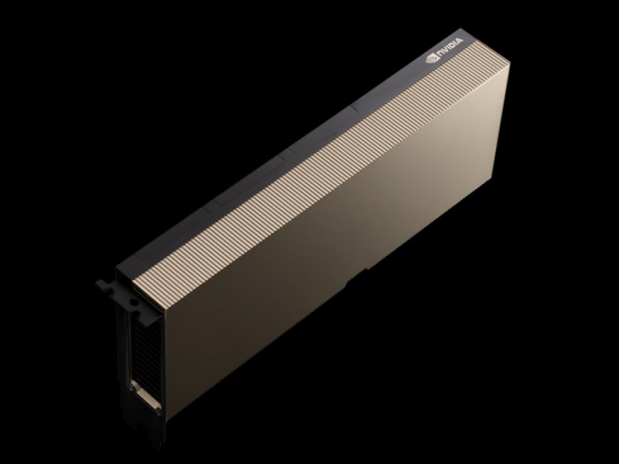
NVIDIA has announced that its launching today its brand new HGX A100 systems that incorporate the updated A100 PCIe GPU accelerators featuring twice the memory & faster bandwidth for HPC users.
The existing NVIDIA A100 HPC accelerator was introduced last year in June and it looks like the green team is planning to give it a major spec upgrade. The chip is based on NVIDIA's largest Ampere GPU, the A100, which measures 826mm2 and houses an insane 54 billion transistors. NVIDIA gives its HPC accelerators a spec boost during mid-cycle which means that we will be hearing about the next-generation accelerators at GTC 2022.
NVIDIA A100 Tensor Core GPUs deliver unprecedented HPC acceleration to solve complex AI, data analytics, model training and simulation challenges relevant to industrial HPC. A100 80GB PCIe GPUs increase GPU memory bandwidth 25 percent compared with the A100 40GB, to 2TB/s, and provide 80GB of HBM2e high-bandwidth memory.
The A100 80GB PCIe’s enormous memory capacity and high-memory bandwidth allow more data and larger neural networks to be held in memory, minimizing internode communication and energy consumption. Combined with faster memory bandwidth, it enables researchers to achieve higher throughput and faster results, maximizing the value of their IT investments.
A100 80GB PCIe is powered by the NVIDIA Ampere architecture, which features Multi-Instance GPU (MIG) technology to deliver acceleration for smaller workloads such as AI inference. MIG allows HPC systems to scale compute and memory down with guaranteed quality of service. In addition to PCIe, there are four- and eight-way NVIDIA HGX A100 configurations.
NVIDIA partner support for the A100 80GB PCIe includes Atos, Cisco, Dell Technologies, Fujitsu, H3C, HPE, Inspur, Lenovo, Penguin Computing, QCT and Supermicro. The HGX platform featuring A100-based GPUs interconnected via NVLink is also available via cloud services from Amazon Web Services, Microsoft Azure and Oracle Cloud Infrastructure.
In terms of specifications, the A100 PCIe GPU accelerator doesn't change much in terms of core configuration. The GA100 GPU retains the specifications we got to see on the 250W variant with 6912 CUDA cores arranged in 108 SM units, 432 Tensor Cores, and 80 GB of HBM2e memory that delivers higher bandwidth of 2.0 TB/s compared to 1.55 TB/s on the 40 GB variant.
The A100 SMX variant already comes with 80 GB memory but it doesn't feature the faster HBM2e dies like this upcoming A100 PCIe variant. This is also the most amount of memory ever featured on a PCIe-based graphics card but don't expect consumer graphics cards to feature such high capacities any time soon. What's interesting is that the power rating remains unchanged which means that we are looking at higher density chips binned for high-performance use cases.
The FP64 performance is still rated at 9.7/19.5 TFLOPs, FP32 performance is rated at 19.5 /156/312 TFLOPs (Sparsity), FP16 performance is rated at 312/624 TFLOPs (Sparsity) and the INT8 is rated at 624/1248 TOPs (Sparsity). NVIDIA is planning to release its latest HPC accelerator next week and we can also expect the pricing of over $20,000 US considering the 40 GB A100 variant sells for around $15,000 US.
In addition to these announcements, NVIDIA has also announced its new InfiniBand solution that provides configurations of up to 2048 points of NDR 400 Gb/s (or 4096 ports of NDR 200) with a total bi-directional throughput of 1.64 Pb/s. That alone is a 5x increase over the previous-gen and offers 32x higher AI accelerator.
What's Your Reaction?


