


Intel Sapphire Rapids-SP Xeon CPUs To Feature 4 8-Hi HBM2E Stacks, 14 EMIB Interconnects, Full XCC Die Measures Around 400mm2
Intel Sapphire Rapids-SP Xeon CPUs To Feature 4 8-Hi HBM2E Stacks, 14 EMIB Interconnects, Full XCC Die Measures Around 400mm2
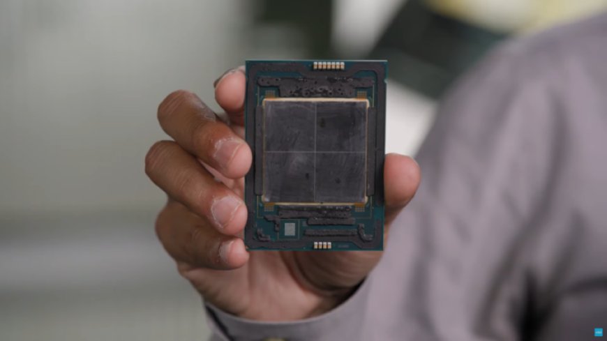
Intel has disclosed the first information regarding its Sapphire Rapids-SP Xeon CPUs which will be featuring HBM2E memory stacks alongside the main core dies in a multi-chiplet design.
We have already detailed Intel's Sapphire Rapids-SP Xeon CPUs earlier but based on the new information published during HotChips 33, it looks like the blue team is disclosing a few more tidbits regarding its next-gen Xeon CPUs.
According to Intel, the Sapphire Rapids-SP will come in two package variants, a standard, and an HBM configuration. The standard variant will feature a chiplet design composed of four XCC dies that will feature a die size of around 400mm2. This is the die size for a singular XCC die and there will be four in total on the top Sapphire Rapids-SP Xeon chip. Each die will be interconnected via EMIB which has a pitch size of 55u and a core pitch of 100u.
The standard Sapphire Rapids-SP Xeon chip will feature 10 EMIB interconnects and the entire package will measure at a mighty 4446mm2. Moving over to the HBM variant, we are getting an increased number of interconnects which sit at 14 and are needed to interconnect the HBM2E memory to the cores.
The four HBM2E memory packages will feature 8-Hi stacks so Intel is going for at least 16 GB of HBM2E memory per stack for a total of 64 GB across the Sapphire Rapids-SP package. Talking about the package, the HBM variant will measure at an insane 5700mm2 or 28% larger than the standard variant. Compared to the recently leaked EPYC Genoa numbers, the HBM2E package for Sapphire Rapids-SP would end up 5% larger while the standard package will be 22% smaller.
Intel also states that the EMIB link provides twice the bandwidth density improvement and 4 times better power efficiency compared to standard package designs.
Intel also detailed the package and die size of its flagship Ponte Vecchio GPU based on the Xe-HPC architecture. The chip will consist of 2 tiles with 16 active dies per stack. The maximum active top die size is going to be 41mm2 while the base die size which is also referred to as the 'Compute Tile' sits at 650mm2. The Ponte Vecchio GPU makes use of 8 HBM 8-Hi stacks and contains a total of 11 EMIB interconnects. The whole Intel Ponte Vecchio package would measure 4843.75mm2. It is also mentioned that the bump pitch for Meteor Lake CPUs using High-Density 3D Forveros packaging will be 36u.
Moving forward, Intel has several next-generation solutions for advanced packaging designs such as Forveros Omni and Forveros Direct as they enter the Angstrom Era of transistor development.
What's Your Reaction?


