


Intel Sapphire Rapid-SP Xeon CPUs To Feature Up To 64 GB HBM2e Memory, Also Talks Next-Gen Xeon & Data Center GPUs For 2023+
Intel Sapphire Rapid-SP Xeon CPUs To Feature Up To 64 GB HBM2e Memory, Also Talks Next-Gen Xeon & Data Center GPUs For 2023+
At SC21 (Supercomputing 2021), Intel hosted a brief session where they discussed their next-generation data center roadmap and talked about their upcoming Ponte Vecchio GPUs & the Sapphire Rapids-SP Xeon CPUs.
Intel had already discussed most of the technical details regarding its next-gen data center CPU & GPU lineup at Hot Chips 33. They are reaffirming what they've said and also revealing a few more tidbits at SuperComputing 21.
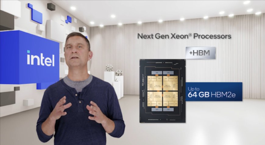
The current generation of Intel Xeon Scalable processors has been extensively adopted by our HPC ecosystem partners, and we are adding new capabilities with Sapphire Rapids – our next-generation Xeon Scalable processor that is currently sampling with customers. This next-generation platform delivers multi-capabilities for the HPC ecosystem, bringing for the first time in-package high bandwidth memory with HBM2e that leverages the Sapphire Rapids multi-tile architecture. Sapphire Rapids also brings enhanced performance, new accelerators, PCIe Gen 5 and other exciting capabilities optimized for AI, data analytics and HPC workloads.
HPC workloads are evolving rapidly. They are becoming more diverse and specialized, requiring a mix of heterogeneous architectures. While the x86 architecture continues to be the workhorse for scalar workloads, if we are to deliver orders-of magnitude performance gains and move beyond the exascale era, we must critically look at how HPC workloads are run within vector, matrix and spatial architectures, and we must ensure these architectures seamlessly work together.Intel has adopted an “entire workload” strategy, where workload-specific accelerators and graphics processing units (GPU) can seamlessly work with central processing units (CPU) from both hardware and software perspectives.
We are deploying this strategy with our next-generation Intel Xeon Scalable processors and Intel Xe HPC GPUs (code-named “Ponte Vecchio”) that will power the 2 exaflop Aurora supercomputer at Argonne National Laboratory. Ponte Vecchio has the highest compute density per socket and per nodes, packing 47 tiles with our advanced packaging technologies: EMIB and Foveros. There are over 100 HPC applications running on Ponte Vecchio. We are also working with partners and customers including – ATOS, Dell, HPE, Lenovo, Inspur, Quanta and Supermicro – to deploy Ponte Vecchio in their latest supercomputers.
via Intel
Intel Sapphire Rapids-SP Xeon Data Center CPUs
According to Intel, the Sapphire Rapids-SP will come in two package variants, a standard, and an HBM configuration. The standard variant will feature a chiplet design composed of four XCC dies that will feature a die size of around 400mm2. This is the die size for a singular XCC die and there will be four in total on the top Sapphire Rapids-SP Xeon chip. Each die will be interconnected via EMIB which has a pitch size of 55u and a core pitch of 100u.
The standard Sapphire Rapids-SP Xeon chip will feature 10 EMIB interconnects and the entire package will measure at a mighty 4446mm2. Moving over to the HBM variant, we are getting an increased number of interconnects which sit at 14 and are needed to interconnect the HBM2E memory to the cores.
The four HBM2E memory packages will feature 8-Hi stacks so Intel is going for at least 16 GB of HBM2E memory per stack for a total of 64 GB across the Sapphire Rapids-SP package. Talking about the package, the HBM variant will measure at an insane 5700mm2 or 28% larger than the standard variant. Compared to the recently leaked EPYC Genoa numbers, the HBM2E package for Sapphire Rapids-SP would end up 5% larger while the standard package will be 22% smaller.
Intel also states that the EMIB link provides twice the bandwidth density improvement and 4 times better power efficiency compared to standard package designs. Interestingly, Intel calls the latest Xeon lineup Logically monolithic which means that they are referring to the interconnect that'll offer the same functionality as a single-die would but technically, there are four chiplets that will be interconnected together. You can read the full details regarding the standard 56 core & 112 thread Sapphire Rapids-SP Xeon CPUs here.
Intel Ponte Vecchio Data Center GPUs
Moving over to Ponte Vecchio, Intel outlined some key features of its flagship data center GPU such as 128 Xe cores, 128 RT units, HBM2e memory, and a total of 8 Xe-HPC GPUs that will be connected together. The chip will feature up to 408 MB of L2 cache in two separate stacks that will connect via the EMIB interconnect. The chip will feature multiple dies based on Intel's own 'Intel 7' process and TSMC's N7 / N5 process nodes.
Intel also previously detailed the package and die size of its flagship Ponte Vecchio GPU based on the Xe-HPC architecture. The chip will consist of 2 tiles with 16 active dies per stack. The maximum active top die size is going to be 41mm2 while the base die size which is also referred to as the 'Compute Tile' sits at 650mm2.
The Ponte Vecchio GPU makes use of 8 HBM 8-Hi stacks and contains a total of 11 EMIB interconnects. The whole Intel Ponte Vecchio package would measure 4843.75mm2. It is also mentioned that the bump pitch for Meteor Lake CPUs using High-Density 3D Forveros packaging will be 36u.
Aside from these, Intel also posted a roadmap in which they confirm that the next-generation Xeon Sapphire Rapids-SP family and the Ponte Vecchio GPUs will be available in 2022 but there's also the next-generation product lineup which is planned for 2023 and beyond. Intel hasn't explicitly told what it plans to bring but we know that Sapphire Rapids successor will be known as Emerald and Granite Rapids and the successor to that will be known as Diamond Rapids.
For the GPU side, we don't know what the successor to Ponte Vecchio will be known but expect it to be competing with NVIDIA's and AMD's next-generation GPUs for the data center market.
Moving forward, Intel has several next-generation solutions for advanced packaging designs such as Forveros Omni and Forveros Direct as they enter the Angstrom Era of transistor development.
What's Your Reaction?


