


Intel Launches Lakefield ‘4+1’ 3D SoC To Take On The Low Power Mobility Market
Intel Launches Lakefield ‘4+1’ 3D SoC To Take On The Low Power Mobility Market
Intel has finally launched its Lakefield platform that houses 5 cores on one 3D package. Consisting of 4 low power Tremont cores and high-performance core, the chip will take on the low power mobility market in just under 7W of power. This is a major innovation from Intel and a packaging technique that is yet unmatched on the market. Whether the company is able to get any design wins, however, remains to be seen. Intel has currently announced two SoCs on the Lakefield platform:
Both SKUs consist of the 4+1 design and feature a 7W TDP along with a 4MB cache. The difference is in the graphics section and the clock speeds. For the flagship SKU, you are looking at 64 EUs that are clocked up to 500 Mhz, and is dubbed the "i5". For the i3 variant, you are looking at 48 EUs clocked at the same speed. The flagship SKU is also clocked at a higher base frequency of 1.4 GHz (compared to 800 Mhz on the i3) and can boost further as well (3.0 GHz vs 2.8 Ghz).
The market Intel is trying to tap into here is predominantly ARM based and could also have something to do with rumors about Apple planning to shift to its in-house designs soon. Intel has a lot of experience in designing these SoCs and considering the tech involved with this product, we are eager to see the reception it gets from OEMs and ODMs. The complete press deck for the Lakefield reveal is given below:
Some press blurbs from Intel official:
“Intel Core processors with Intel Hybrid Technology are the touchstone of Intel’s vision for advancing the PC industry by taking an experience-based approach to designing silicon with a unique combination of architectures and IPs. Combined with Intel’s deepened co-engineering with our partners, these processors unlock the potential for innovative device categories of the future.” –Chris Walker, Intel corporate vice president and general manager of Mobile Client Platforms
Why They’re Great for Innovative PC Form Factors: Intel Core processors with Intel Hybrid Technology deliver full Windows 10 application compatibility in up to a 56% smaller package area for up to 47% smaller board size1 and extended battery life, providing OEMs more flexibility in form factor design across single, dual and foldable screen devices while delivering the PC experiences people expect. They are also:
About Key Features & Capabilities: Intel Core i5 and i3 processors with Intel Hybrid Technology leverage a 10nm Sunny Cove core to take on more intense workloads and foreground applications, while four power-efficient Tremont cores balance power and performance optimization for background tasks. The processors are fully compatible with 32- and 64-bit Windows applications, helping reach new heights for the thinnest and lightest designs.
Here is what the official description for the Intel Tremont reads:
The Tremont CPU architecture was designed for enhanced processing power in compact, low power packages. Products based on Tremont will span both client, IOT and Data Center products and combined with broader Intel portfolio of IPs Tremont will power a new generation of Intel products across the compute offering. This presentation will unveil, for the first time publicly, the details of the micro-architecture of Tremont as well as briefly touch on the implementation of Tremont with other Intel compute cores.
Intel's Tremont instruction set will feature a Core-standard branch prediction as well as 6 wide out of order instruction decode with 4 wide allocations. All of this will be connected by 10 execution ports and an L2 cache up to 4.5MB. The end product is a product that roughly offers Sandy Bridge level of performance in a highly mobile and portable package. Intel is focusing significantly on the single-thread performance this time and showed off some single-thread performance improvement graphs (SPECint* Rate base) relative to Goldmont Plus.
The performance hybrid part of the Tremont cores is something we have already tackled before in the Lakefield platform overview. The power/performance graphs definitely mirror Sunny Cove but features much higher power efficiency at much lower performance levels. The result is a core that will significantly improve battery life even when the "little" cores are engaged. Sunny Cove is set to be the biggest update in Intel's lineup and both of these products will be manufactured on the 10nm process.
[Read more here. ]
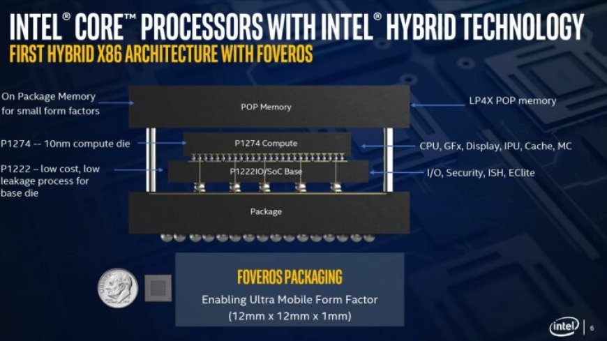
Talking about the SOC itself and its individual layers, the Lakefield SOC that has been previewed consists of at least four layers or dies, each serving a different purpose. The top two layers are composed of the DRAM which will supplement the processor as the main system memory. This is done through the PoP (Package on Package) memory layout which stacks two BGA DRAMs on top of each other as illustrated in the preview video. The SOC won't have to rely on socketed DRAM in this case which saves a lot of footprint on the mainboard.
The second layer is the Compute Chiplet with a Hybrid CPU architecture and graphics, based on the 10nm process node. The Hybrid CPU architecture has a total of five individual Cores, one of them is labeled as the Big Core which features the Sunny Cove architecture. That's the same CPU architecture that will be featured on Intel's upcoming 10nm Ice Lake processors. The Sunny Cove Core is optimized for high-performance throughput. There are also four small CPUs that are based on the 10nm process but optimized for power efficiency.
The same die consists of Intel's Gen 11 graphics engine with 64 Execution Units. Last week, we got to see the performance of an Intel GT2 (Gen 11) Iris Plus 940 graphics chip with 64 Execution Units and the results were quite good compared to existing Intel Gen 9.5 graphics chips. You can check out the performance results here.
Knowing that the Lakefield SOC will feature the same graphics engine, we can expect a very decent graphics performance out of this 3D stacked processor. Then last of all is the base die which serves as the cache and I/O block of the SOC. Labeled as the P1222 and based on a 22FFL process node, the base die comes with a low cost and low leakage design while providing a feature-rich array of I/O capabilities.
What's Your Reaction?


