


Intel Core Ultra “Meteor Lake” CPU Die Shots Give A Closer Look At Various CPU, GPU & IO Chiplets
Intel Core Ultra “Meteor Lake” CPU Die Shots Give A Closer Look At Various CPU, GPU & IO Chiplets
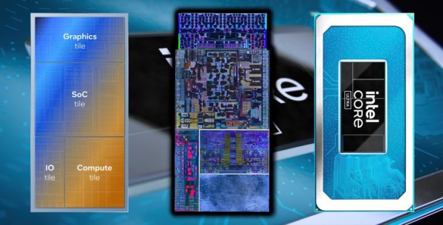
Intel's Core Ultra "Meteor Lake" CPUs have received their first die shots which give us a closer look at the different IPs incorporated within the chiplets.
The die shots were posted by HXL (@9559pro) and give us a better look at the chiplet (Tile) layout of the Meteor Lake CPUs versus the 3D renders published by Intel. As we know from our deep dive, the Intel Core Ultra "Meteor Lake" CPUs are based on a disaggregated architecture that is used to combine various IPs on a singular package in a chiplet-esque fashion. For Meteor Lake, there are a total of four chiplets which include a Compute (CPU), Graphics (GPU), SOC (NPU, etc), and I/O tiles.
All four tiles will utilize internal and external fabrication processes which means that some of the tiles will be made by Intel while the rest will be made by 3rd party fabs such as TSMC. The main CPU tile will be using the "Intel 4" or 7nm EUV process node while the SOC Tile and IOE Tiles will be fabricated on TSMC's 6nm process node (N6). Intel calls Meteor Lake the first step into the chiplet ecosystem in the client segment. The tGPU which is a new name for the iGPU (Tiled-GPU) is also a major component of Meteor Lake CPUs and utilizes TSMC's 5nm process node. So to quickly sum it all up:
Meteor Lake Full Die Shot (Image Credits: HXL via QQ):
The die-shots were taken from a 2+8+2 SKU which includes 2 P-Cores based on the Redwood Cove, 8 E-Cores based on the Crestmont, and 2 additional but low-power E-Cores based on the very same Crestmont E-Cores. The first 2 P-Cores and 8 E-Cores reside within the Compute (CPU) tile and here you can see the two large P-Cores on the top followed by the smaller 8 E-Cores at the bottom.
The large blocks in the middle are the cache. In the case of this configuration, there is a total of 12 MB of Smart Cache with the Redwood Cove P-Cores feature 2 MB L2 per core, and the Crestmont E-Cores pack 4 MB of L2 cache per cluster. This pretty much falls in line with what Locuza had stated earlier in his die-shot analysis.
Moving over the GPU tile, we have a 4 Xe-Core variant based on the Arc Akchemist architecture while the most jam-packaged sections seem to be the SOC and I/O tile which have various parts such as controllers (Memory/Storage/PCIe), NPUs, a dedicated low-power island for Video & a lot more. The SOC tile has the two Crestmont LP E-Cores.
Meteor Lake SOC Tile (Image Credits: HXL via QQ):
Meteor Lake IOE Tile (Image Credits: HXL via QQ):
In addition to the whole die shot, we also get a look at a dummy spacer die on this configuration which is something that was showcased in recently revealed Thermal Test Dies for Intel Core Ultra "Meteor Lake" CPUs. Some people confused the two split Compute (Tiles) as a chip with a higher core count than what's available in current Meteor Lake SKUs but that isn't the case. That die was specifically designed to test both 2+8 and 6+8 SKU configurations in thermal envelope tests while you can see that 2+8 dies have almost half the area empty which only serves as a dummy die.
MeteorLake-P:-Normal Sample DieandThermal test Sample Die pic.twitter.com/Laxft2dodm
— 结城安穗-YuuKi_AnS (@yuuki_ans) December 18, 2023
Some die size analysis from OneRaichu & Andreas Schilling reveals that the Compute (Tile) should measure around 69.67mm2 (8.72*7.99 mm), SOC tile measures around 100.15mm2 (10.85*9.23 mm), GPU tile measures around 44.25mm2 (10.22*4.33 mm) and the IO tile measures around 27.42mm2 (9.20*2.98 mm).
For comparison purposes, the AMD Zen 4 CCD with 8 cores and 32 MB of L3 cache measures 66.3 mm2 which is around 5% smaller than the Meteor Lake compute tile. Overall, the die shots look a lot more interesting than the 3D renders and we can't see annotated versions to be released soon.
What's Your Reaction?


