


Development Of Intel’s 1.8nm & 2nm Process Nodes Completed, Expected First Half of 2024
Development Of Intel’s 1.8nm & 2nm Process Nodes Completed, Expected First Half of 2024
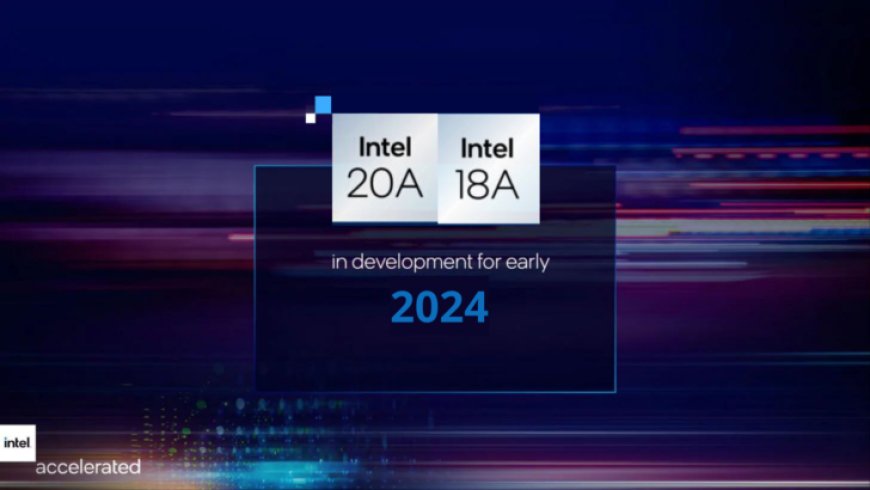
Intel has reportedly finished the development of its planned 18A & 20A fabrication processes that will be used internally and by Intel Foundry Services (IFS) clients. The new 1.8nm and 2nm process nodes will be ready for manufacturing as soon as the first half of next year.
Now that the company has finalized the specifications of the new process node technologies, Intel can begin to determine when the two fabrication processes will begin production during the first half of 2024.
We have an active pipeline of engagements with seven out of the 10 largest foundry customers coupled with consistent pipeline growth to include 43 potential customers and ecosystem partner test chips. Additionally, we continue to make progress on Intel 18A, and have already shared the engineering release of PDK 0.5 (process design kit) with our lead customers and expect to have the final production release in the next few weeks.
— Pat Gelsinger, Chief Executive Officer, Intel
The 18A and 20A (the "A" standing for "angstroms") will utilize new technologies beginning with the 20A's use of RibbonFET transistors. This introduction of RibbonFET and PowerVia will accelerate backside power delivery, with the company anticipating that it will surpass its competitors in the semiconductor fabrication processes. The two most significant competitors for Intel now are Samsung and TSMC.
Intel's 18A process will build off of the 20A process by reducing the size of the transistor while maintaining the power of the process node. The original set time frame the company selected for this introduction was 2025. The company has adjusted the release to the second half of 2024.
Intel also changed the utilization of the ASML Twinscan EXE scanners for developing the 18A process node to the current Twinscan NXE scanners. The difference between the two machines is that the latter uses 0.33 numerical aperture (NA) optics to develop the process nodes, while the former uses 0.55 NA optics. Additionally, Intel will utilize extreme ultraviolet (EUV) double patterning lithography.
It is unknown what chip series 18A will be incorporated within, but the company has officially confirmed that the 20A process technology will be used for the codename "Arrow Lake." Intel 18A is shown to be incorporated into future client-based "Lake" series chips, "Rapids" series data center chipsets, and foundry chips for Intel clients.
It is also reported that Intel has already produced the first test chips on the 20A and 18A process nodes, but it is not mentioned if these chips are internally designed by Intel or for a 3rd party client.
News Source: Tom's Hardware
What's Your Reaction?


