


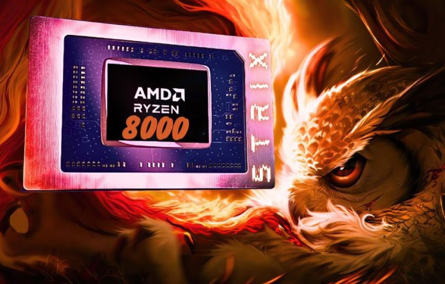
AMD Ryzen 8000 “Strix Point” APU Sample Allegedly Spotted: 12 Core Hybrid Zen 5 Design In A 45W TDP
AMD Ryzen 8000 “Strix Point” APU Sample Allegedly Spotted: 12 Core Hybrid Zen 5 Design In A 45W TDP
An alleged AMD Ryzen 8000 "Strix Point" APU sample has been unearthed by Performance Databases, featuring 12 Hybrid Zen 5 cores.
We know quite a fair bit about AMD's Ryzen 8000 "Strix Point" APUs which will be the follow-on to Phoenix 2 chips featuring a hybrid core design. Unlike Intel's implementation of P-Cores & E-Cores, the AMD hybrid design will make use of standard Zen and the compute-density optimized Zen "C" cores. The difference between those and the E-Cores is that they offer the same ISA and also carry support for hyper-threading while retaining the same clock speeds.
So coming to the alleged chip that has leaked out, Performance Databases posted two pictures, a CPU-z & an HWiNFO screenshot of the AMD Ryzen 8000 "Strix Point" APU sample. The same being super early is not correctly identified by either software. CPU-z reads it as an AMD Eng Sample with clocks running at 3.0 GHz and a single-core chip whereas HWiNFO provides some better data with a 12-core design arranged in a 4+8 configuration.
The AMD Ryzen 8000 "Strix Point" APUs sample carries 4 cores and 8 threads based on the Zen 5 core architecture while the other 8 cores and 16 threads are based on the Zen 5C architecture. It comes in a 45W TDP package and is built upon a 4nm process node (from TSMC). As for the cache, the Zen 5 cores carry 48 KB L1 Instruction and 32 KB L1 instruction cache, 4 MB L2 cache per core (for Zen 5) and 2 MB L2 cache per core (for Zen 5C) and 8 MB L3 cache (Shared across all cores). It provides the chip with 32 MB of L2 cache.
The clock speeds are messy since the software doesn't seem to report them correctly as there's no way the chip will have clocks above 6 GHz but that's all the info about this particular chip and SKU available now.
For the iGPU side, the AMD Ryzen 8000 "Strix Point" APUs will be configured with the AMD RDNA 3.5 GPU cores with 8 WGP's (Work Group Processors) and a total of 16 Compute Units for up to 1024 stream processors. That's a 33% increase in the number of stream processors and if clock speeds will remain the same at around 2.8-3.0 GHz range, we can expect up to 12 TFLOPs FP32 compute horsepower which will mark a 42% increase over the current fastest RDNA 3 iGPU, the Radeon 780M.
The AMD Strix Point APUs are expected to arrive in 2024 which means they will be competing with Intel's Arrow Lake and the follow-up, Lunar Lake. Intel is also going to be implementing similar tech such as hybrid cores, chiplets, and increased graphics cores within its future disaggregated lineup so it will be a very interesting competition between the two adversaries, mainly within the mobile and laptop segment.
What's Your Reaction?


