


AMD Provides First Look At Aldebaran “CDNA 2” Instinct MI200 Series MCM GPU Block Diagram
AMD Provides First Look At Aldebaran “CDNA 2” Instinct MI200 Series MCM GPU Block Diagram
AMD has offered some further insight on its CDNA 2 "Aldebaran" GPU-powered Instinct MI200 series which are the first to feature an MCM design. The Instinct MI200 GPUs have been detailed by AMD Architects, Alan Smith & Norman James, during Hot Chips 34.
AMD is officially the first to MCM technology and they are doing so with a grand product which is their Instinct MI200 codenamed Aldebaran. The AMD Aldebaran GPU will come in various forms & sizes but it's all based on the brand new CDNA 2 architecture which is the most refined variation of Vega. Some of the main features before we go into detail are listed below:
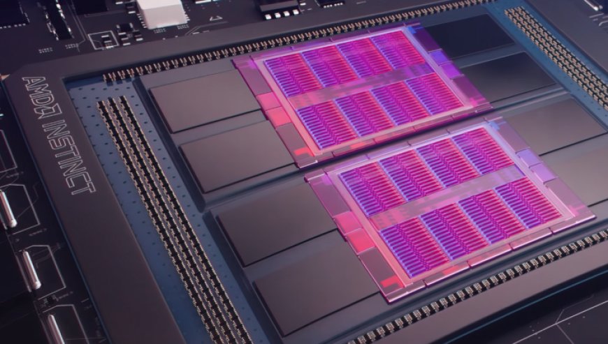
AMD Instinct MI200 GPU Die Shot:
Inside the AMD Instinct MI200 is an Aldebaran GPU featuring two dies, a secondary and a primary. It has two dies with each consisting of 8 shader engines for a total of 16 SE's. Each Shader Engine packs 14 CUs with full-rate FP64, packed FP32 & a 2nd Generation Matrix Engine for FP16 & BF16 operations. The whole GPU is fabricated on TSMC's 6nm process node and comes packed with a total of 58 Billion transistors.
AMD Instinct MI200 GPU Block Diagram:
Each die, as such, is composed of 112 compute units or 7,168 stream processors. This rounds up to a total of 224 compute units or 14,336 stream processors for the entire chip. The Aldebaran GPU is also powered by a new XGMI interconnect. Each chiplet features a VCN 2.6 engine and the main IO controller. Each GPU chiplet has four 1024-bit memory controllers for the HBM2e memory.
As for the cache, each GPU chiplet features a total of 8 MB of L2 capacity which is physically partitioned into 32 slices. Each slice delivers 128B/CLK with enhanced queuing and arbitration plus enhanced atomic operations. The per GCD memory subsystem includes 64 GB of HBM2e memory per chiplet with an aggregated 1.6 TB/s of bandwidth per GCD which is partitioned into 32 channels with a 64B/CLK for efficient operational voltage. The in-Package interconnect includes a 400 GB/s bi-sectional bandwidth across the two GCDs.
There are a total of 8 Infinity Fabric interconnects of which one on each GPU can be used for PCI-Express interconnect. The interconnect is rated at a coherent CPU-GPU transfer rate of 144 GB/s. You can scale up to 500 GB/s using the external Infinity Fabric link with a total of four MI200 series GPUs or scale out using a PCIe Gen 4 ESM AIC for 100 GB/s bandwidth.
AMD Instinct MI200 "Aldebaran GPU" Performance Metrics:
In terms of performance, AMD is touting various record wins in the HPC segment over NVIDIA's A100 solution with up to 3x performance improvements in AMG.
As for DRAM, AMD has gone with an 8-channel interface consisting of 1024-bit interfaces for an 8192-bit wide bus interface. Each interface can support 2GB HBM2e DRAM modules. This should give us up to 16 GB of HBM2e memory capacity per stack and since there are eight stacks in total, the total amount of capacity would be a whopping 128 GB. That's 48 GB more than the A100 which houses 80 GB HBM2e memory. The memory will clock in at an insane speed of 3.2 Gbps for a full-on bandwidth of 3.2 TB/s. This is a whole 1.2 TB/s more bandwidth than the A100 80 GB which has 2 TB/s.
The AMD Instinct MI200 CDNA 2 "Aldebaran" GPUs are already powering the world's fastest super-computer, the Frontier, which is also the world's first Exascale machine, offering 1.1 ExaFLOPs of compute horsepower and currently listed at the top within the TOP500 and Green500 lists. AMD has also unveiled its future plans for the Instinct MI300 APU lineup which will further leverage the chiplet architecture and take things to the next level.
What's Your Reaction?


