


218-Layer 3D NAND Flash From Kioxia & Western Digital Delivers Huge Leap In Performance & Cost Effectiveness
218-Layer 3D NAND Flash From Kioxia & Western Digital Delivers Huge Leap In Performance & Cost Effectiveness
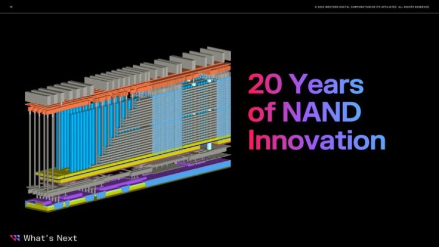
Kioxia & Western Digital Corp. (WD) revealed their newest 218-layer 3D NAND flash memory technology which delivers a huge performance uplift. The new 3D flash memory technology incorporates larger capacity and reliability with a performance boost. The companies also did their best to make the new technology more pleasing in cost.
Kioxia and WD utilize advanced scaling and wafer bonding techniques to make them excellent for meeting the demands of exponential data growth across several market segments. The two companies lowered costs by introducing several distinctive processes and architectures, promoting continued lateral scaling advances.
Vertical and lateral scaling delivers higher capacity levels in a smaller die area with fewer layers needed at a more enticing cost to the client. The technology is similar to YMTC's Xtacking technology, which is in its third generation. YMTC Xtacking 3.0 is the company's 3D NAND architecture involving bonding a CMOS wafer with a memory cell wafer. Xtacking 3.0 introduced back-side source connect (BSSC) for memory cell wafers, leading to simpler processes and lower costs.
The new 3D flash memory demonstrates the benefits of our strong partnership with Kioxia and our combined innovation leadership. By working with one common R&D roadmap and continued investment in R&D, we have been able to productize this fundamental technology ahead of schedule and deliver high-performance, capital-efficient solutions.
— Alper Ilkbahar, Senior Vice President of Technology & Strategy, Western Digital
Kioxia and WD also produced next-generational CMOS directly Bonded to Array (CBA) technology. Each CMOS wafer and cell array wafer is created individually, albeit optimized, and then joined together to deliver increased bit density and faster NAND input and output speeds.
Through our unique engineering partnership, we have successfully launched the eighth-generation BiCS FLASHTM with the industry's highest1 bit density. I am pleased that Kioxia’s sample shipments for limited customers have started. By applying CBA technology and scaling innovations, we’ve advanced our portfolio of 3D flash memory technologies for use in various data-centric applications, including smartphones, IoT devices, and data centers.
— Masaki Momodomi, Chief Technology Officer, Kioxia Corporation
The new 218-layer 3D flash will leverage 1 TB triple-level-cell (TLC) and quad-level-cell (QLC) with four planes and showcase brand-new lateral shrink technology to improve bit density by over fifty percent. The high-speed NAND I/O by Kioxia and WD is set at over 3.2Gb/s, which is a sixty percent improvement over previous generations, and increases the write performance and read latency by twenty percent to ramp up usability and performance.
News Source: Business Wire
What's Your Reaction?


